


Photo Mask
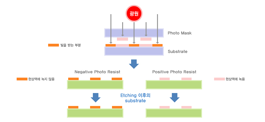
What is Photo Mask
It is used as a very important raw material in the production of semiconductor chips and displays and it is the projection of a pattern designed onto to blank mask.
In other words, it enables a manufacturer to expose the patterns using the photomasks directly onto wafers and circuit boards playing a role much like a film inside a camera.
In other words, it enables a manufacturer to expose the patterns using the photomasks directly onto wafers and circuit boards playing a role much like a film inside a camera.
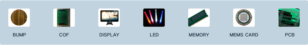
Application
Nozzle Wusing Photo Mask